SUSS MicroTec
MA 6 BA 6 Mask
The SUSS MicroTec MA 6 BA 6 Mask is a mask aligner. The SUSS MicroTec MA 6 BA 6 Mask provides front-side and backside alignment. The SUSS MicroTec MA 6 BA 6 Mask supports alignment on individual die up to six-inch wafers.[1]

Wafer size
Wafer chuck (1)
Power
200-240 V[2]
Vacuum
Soft, Hard, Vacuum[4]
Performance
Supported[4]
Optics
5x ,10x , 20x[4]
What it is
The SUSS MicroTec MA 6 / BA 6 is a contact mask aligner used for photolithography. The machine is designed for front-side and back-side alignment exposure of substrates. The system combines the MA 6 mask aligner role with the BA 6 bond aligner or back-side alignment configuration. The MA 6 / BA 6 supports wafer sizes from 2 to 6 inches. The equipment is part of the mature-node lithography tool class used in research, development, and small-volume production.[2][3][4][9][1]
Some units are configured with top-side alignment (TSA) and back-side alignment (BSA) capability. Configurations may include an optical BSA system, a DVM6 microscope, and UV400 optics that support exposure wavelengths of 365 nm and 405 nm. Objectives of 5x, 10x, and 20x are used with the alignment microscope. The system can operate in soft, hard, and vacuum contact modes depending on tooling. A 350 W lamphouse and a Generation 2 CIC power supply are used on typical systems. The tool operates on 230 V, 50/60 Hz supply with a nominal load of 1500 VA in some configurations.[4][9][3]
Where it fits in the process flow
The MA 6 / BA 6 sits at the lithography step in a micro-fabrication process flow. Photolithography using a mask aligner defines the pattern that is later etched, implanted, or deposited onto the substrate. Contact lithography is typically used for feature sizes that are larger than those produced by projection steppers, and it is common in MEMS, microfluidics, and compound semiconductor fabrication. The tool is used for patterning individual die as well as full wafers.[1]
In a typical process, the substrate is first cleaned and coated with photoresist, then loaded onto the aligner chuck. After alignment and exposure, the substrate moves to a develop step, followed by etching or other pattern transfer processes. The tool may be paired with wafer bonding equipment, since the back-side alignment capability allows patterns on one wafer to be aligned to features on the back side of another wafer before bonding.[1]
Applications
The MA 6 / BA 6 is used for contact photolithography in research and production environments. The tool is used for patterning of MEMS devices, microfluidic structures, and other microsystems. The back-side alignment capability supports double-sided lithography, which is important for devices that require patterns on both sides of a substrate. The system can also be used for compound semiconductor and silicon device fabrication.[1][4]
Applications include patterning of photoresist for subsequent etching, electroplating, or liftoff processes. The wafer bonding context is a notable application, since the aligner works with bonders to align wafers before bonding. The support for substrates up to 6 inches makes the tool suited for small-format production and prototyping.[1][4]
What do the numbers mean?
Power & electrical9
Vacuum & pumping2
- Capable of Soft, Hard, and Vacuum contact modes (tooling-dependent)[4]
Wafer handling3
Optics & imaging8
Performance4
- TSA (Top-Side Alignment), BSA (Back-Side Alignment)[3]
Control & software2
- HDD and software included[4]
Configuration & options20
Vintage & configurations
Documented models & variants
| Designation | Generation | Vintage | Changes | Source |
|---|---|---|---|---|
| MA 6 / BA 6 TSA (Top-Side Alignment), BSA (Back-Side Alignment) | — | 2001 | Listed with TSA and BSA. | Equipment inventory listing[3] |
| MA 6 / BA 6 Optical BSA | — | 2000 | Listed with optical BSA, DVM6 microscope, upgraded Gen2 CIC power supply, 350W lamphouse, 50/60 Hz, 230 V, and 1500 VA. | Equipment inventory listing[9] |
| MA 6 / BA 6 | — | — | — | Equipment inventory listing[2] |
What does it need to run?
Site utility requirements, footprint, and infrastructure needed to install and operate this tool. Sourced from public records.
- Configuration200-240 V[2]
- Configuration50/60 Hz[2]
- ConfigurationGen2 CIC power supply[4]
- ConfigurationCapable of Soft, Hard, and Vacuum contact modes (tooling-dependent)[4]
- System power230 V, 50/60 Hz[4]
- ConfigurationUpgraded Gen2 CIC Power Supply[9]
- Voltage230 V[9]
- System power230 V, 50/60 Hz, 1500 VA[9]
- Power supplyGen2 CIC power supply[4]
- Contact modesSoft, Hard, Vacuum[4]
- Voltage range200-240 V[2]
Where are the manuals?
Generated from public-source data on file. Enter your email to access — nothing is published; details are routed privately.
Not publicly documented
Field notes
No research found yet — worked with this tool? Share what you know.
Frequently asked questions
What wafer sizes does the MA 6 / BA 6 support?
The MA 6 / BA 6 supports wafer sizes from 2 to 6 inches.[4]
What alignment capabilities are available on the MA 6 / BA 6?
The system supports top-side alignment (TSA) and back-side alignment (BSA). Some units include optical BSA.[3][9]
What exposure wavelengths does the MA 6 / BA 6 optics support?
The UV400 optics support exposure at 365 nm and 405 nm.[4]
What contact modes are available on the MA 6 / BA 6?
The system is capable of soft, hard, and vacuum contact modes, dependent on tooling.[4]
Not publicly documented
The following facts about the MA 6 BA 6 Mask are absent from this record as of this revision. First-hand knowledge or a citation closes a gap; every submission is reviewed before publication.
No publicly documented production dates or lifecycle milestones (introduction, end of production, EOL) for the MA 6 BA 6 Mask are on record.
Answerable by: OEM historical records or a trade-press announcement
The control-system platform and OS era of the MA 6 BA 6 Mask are not on record.
Answerable by: an engineer who operated it or OEM installation records
No publicly documented failure modes or field errata for the MA 6 BA 6 Mask are on record.
Answerable by: a field service engineer, process engineer, or maintenance technician
The process node or technology generation of the MA 6 BA 6 Mask is not on record.
Answerable by: an OEM datasheet or a fab qualification report
No publicly documented compatible parts, consumables, or accessories for the MA 6 BA 6 Mask are on record.
Answerable by: an OEM parts catalog or a service engineer
No research found yet — worked with this tool? Share what you know.
Sources & citations
Sources (10)Every fact above is drawn from these public sources
- [1]MNTC - Equipment and Facilities | Service Centers — louisville.edulouisville.edu
- [2]Inventory photo
- [3]Inventory photo
- [4]Inventory photo
- [5]Inventory photo
- [6]Inventory photo
- [7]Inventory photo
- [8]Inventory photo
- [9]inventory listing
- [10]Mask/bond aligner:front/back capable [SUSS-align] | Quantum-Nano Fabrication and Characterization Facility | University — uwaterloo.cauwaterloo.ca
Last updated Oct 10, 2026.
Compare with similar tools
View all →Brooks 017-0146-01 is a prealigner manufactured by Brooks.
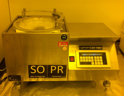
The CEE 100 is a lithography spin coater/developer tool that accepts up to 6-inch wafers and supports programmable multi-step processing.