Veeco
Nexus IBE350
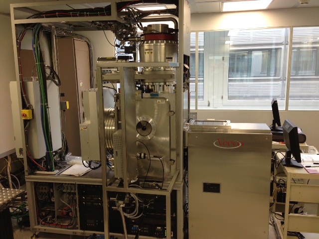
The Veeco Nexus IBE350 is a broad-beam ion etcher. The Veeco Nexus IBE350 uses a 350 mm argon ion source. The Veeco Nexus IBE350 includes a SIMS system for real-time end-point detection.[1]
What it is
The Veeco Nexus IBE350 is a broad-beam ion etcher used for physical sputter etching of materials in semiconductor and microelectronics fabrication.[1]
The system is designed for etching materials that are difficult to process with conventional plasma-based etching, including piezo and ferro electrics, magnetic materials, III-V semiconductors, ohmic metals, and hard mask materials.[1]
How it works
The Nexus IBE350 generates a mono-energetic beam of argon ions using an inductively coupled plasma (ICP) source with a 350 mm diameter quartz vessel and an RF generator operating at 1.8 MHz with a maximum power of 2 kW.[1]
Ion beam extraction and collimation are achieved through a three-grid molybdenum electrostatic optics system. The grids are biased to extract, accelerate, and collimate the ions, while a decelerator grid at ground potential reduces beam divergence and prevents electron back-streaming from the neutralizer.[1]
A plasma bridge neutralizer downstream of the optics emits electrons to prevent space or surface charging of the substrate. A mechanical shutter between the optics and the process chamber allows beam stabilization before etching begins.[1]
A secondary ion mass spectroscopy (SIMS) system collects and analyzes secondary ions ejected from the sample surface, providing real-time end point detection during the etch process.[1]
Where it fits in the process flow
The Nexus IBE350 is employed in process flows where ion beam etching is required, typically after photolithographic patterning and before subsequent deposition or metrology steps. The system processes wafers or substrates mounted on the cooled, rotating fixture.[1]
Because the etch mechanism is purely physical sputtering with no chemical dependence, the IBE350 can be used for materials that are resistant to reactive plasma etch chemistries, such as noble metals, and for processes where anisotropic profiles or low ion damage are critical.[1]
Applications
The system is used for etching piezo and ferro electric materials, magnetic materials, III-V semiconductors (GaAs, InP, GaN, AlN), ohmic metals (Au, Pt, Cu, Ir), and hard mask materials (Ag, TiWN, Ni). The broad energy range from 50 V to 800 V supports processes from low-damage etching to high-rate removal.[1]
The high vacuum capability (base pressure in the 10⁻⁷ mbar range) and the use of pure physical sputtering eliminate chamber contamination and memory effects, making the system suitable for processes requiring high cleanliness and material isolation.[1]
- Etching piezoelectric materials
- Etching ferroelectric materials
- Etching magnetic materials
- Etching III-V materials such as GaAs, InP, GaN, and AlN
- Etching ohmic metals such as Au, Pt, Cu, and Ir
- Etching hard mask materials such as Ag, TiWN, and Ni
- Angular etch and shape control of complex structures
What do the numbers mean?
Power & electrical11
Vacuum & pumping4
Wafer handling8
Gas & chemistry1
Optics & imaging8
Control & software2
Dimensions & facilities1
Configuration & options17
What does it need to run?
Site utility requirements, footprint, and infrastructure needed to install and operate this tool. Sourced from public records.
- Ion source350 mm diameter Argon ion source with RF plasma generator[1]
- RF plasma generator frequency1.8 MHz[1]
- RF plasma generator maximum power2 kW[1]
- Energy range50 V to 800 V[1]
- Operating pressure10^-4 mbar[1]
- Base pressure10^-7 mbar[1]
- RF generator frequency1.8 MHz[1]
- RF generator power2 kW maximum[1]
- Beam energy range50 V to 800 V[1]
- Base pressure10⁻⁷ mbar[1]
- Operating pressure10⁻⁴ mbar[1]
- RF frequency1.8 MHz[1]
- RF power2 kW maximum[1]
- Ion energy range50 V to 800 V[1]
- Ion source typeICP source, 350mm diameter, RF plasma generator, 1.8MHz, 2kW maximum[1]
- Process gasargon[1]
Where are the manuals?
Generated from public-source data on file. Enter your email to access — nothing is published; details are routed privately.
Not publicly documented
Field notes
No research found yet — worked with this tool? Share what you know.
Frequently asked questions
What type of ion source does the Nexus IBE350 use?
The Nexus IBE350 uses an inductively coupled plasma (ICP) source with a 350 mm diameter argon ion source.[1]
What is the beam energy range of the tool?
The beam energy can be set from 50 V to 800 V.[1]
What is the maximum substrate temperature during etching?
The substrate fixture is kept at temperatures below 90 °C.[1]
What tilt angle range is supported?
The tilt angle can be adjusted from +90° to -70°.[1]
Not publicly documented
The following facts about the Nexus IBE350 are absent from this record as of this revision. First-hand knowledge or a citation closes a gap; every submission is reviewed before publication.
No publicly documented production dates or lifecycle milestones (introduction, end of production, EOL) for the Nexus IBE350 are on record.
Answerable by: OEM historical records or a trade-press announcement
No publicly documented variants, configuration options, or revision breakpoints of the Nexus IBE350 are on record.
Answerable by: an OEM product catalog or an engineer who ordered or specified the tool
The control-system platform and OS era of the Nexus IBE350 are not on record.
Answerable by: an engineer who operated it or OEM installation records
No publicly documented failure modes or field errata for the Nexus IBE350 are on record.
Answerable by: a field service engineer, process engineer, or maintenance technician
The process node or technology generation of the Nexus IBE350 is not on record.
Answerable by: an OEM datasheet or a fab qualification report
No research found yet — worked with this tool? Share what you know.
Sources & citations
Sources (1)Every fact above is drawn from these public sources
- [1]epfl.ch — epfl.chepfl.ch
Last updated Oct 8, 2026.
Compare with similar tools
View all →The Applied Materials 0010-47763 is an electrostatic chuck (ESC) assembly used in semiconductor etching processes.
The Applied Materials 0010-16392 is an electrostatic chuck assembly designed for 300 mm wafer processing, featuring a dual electrode configuration.
Oxford Instruments 100 ICP Fluorine is an inductively coupled plasma etcher for fluorine-based etching, supporting cryo DRIE and multiple etch gases including SF6 and C4F8.
